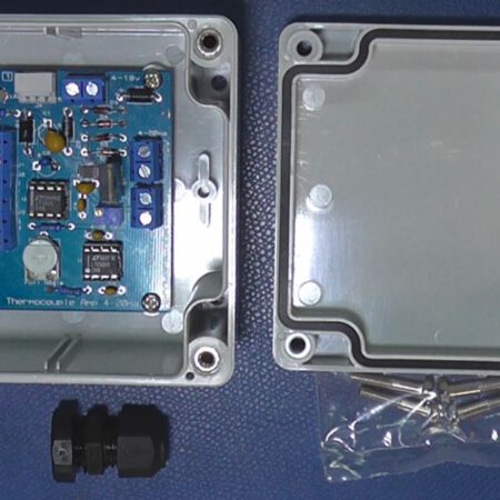
HOW CMOS WORKS: MOSFETS, JFETS, IGFETS AND MORE

CMOS opened the door for many if not most of the properties needed for today’s highly integrated circuits and low power portable and mobile devices. This really couldn’t happen until the speeds and current drive capabilities of CMOS caught up to the other technologies, but catch up they did.
Nowadays CMOS Small Scale Integration (SSI) logic families, I.E. the gates used in external logic, offer very fast speeds and high current drive capability as well as supporting the low voltages found in modern designs. Likewise the Very Large Scale Integration (VLSI) designs, or Very Very Large Scale if you like counting the letter V when talking, are possible due to low power dissipation as well as other factors.
HOW CMOS IS DESIGNED
CMOS, which means Complementary Metal Oxide Semiconductor, is based on combining two polarities of MOSFETS; Metal Oxide Semiconductor Field Effect Transistors.
 Regular transistors, known as Bipolar Junction Transistors (BJT) meaning that they are made from junctions that have a positive and a negative (PN) junction utilize current as the input and create gain by controlling output current. As all of these current flows add up it means that at the end of the day there is a lot of current flowing which results in power being dissipated which ultimately results in heat.
 The Junction Field Effect Transistor (JFET) utilizes voltage instead of current on its Gate input, somewhat like the Base on a Bipolar Transistor, to control the output voltage. Since the Gate is not insulated from the other terminals, known as the Source and Drain, there is a leakage current in JFETs that would not be present if the Gate was insulated from the Source and Drain.
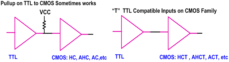
Enter the Insulated Gate FET (IGFET) which is the basis for most of the transistor devices found on large scale integrated chips today. Looking at the diagram, the MOSFETs all show a distinct space between the Gate and the rest of the structure. The other two pins are the Source and the Drain.
Read more at Hackaday.com